400-9988-118

|
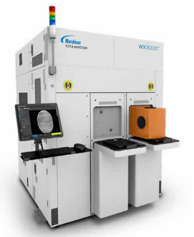
For Semiconductor Wafer-Level & Advanced Packaging WX3000 3D and 2D metrology and inspection systems provide the ultimate combination of high speed, high resolution and high accuracy for wafer-level and advanced packaging applications to improve yields and productivity. Powered by MRS Offering an unparalleled combination of high accuracy, high resolution and speed, MRS sensors are widely used for inspection and measurement in the SMT and semiconductor markets. Nordsons’unique sensor architecture simultaneously captures and transmits multiple images in parallel while proprietary 3D fusing algorithms which merge the images together. The result is ultra-high quality 3D images and high-speed inspection. The 3-micron NanoResolution (X/Y resolution of 3 micron, Z resolution of 50 nanometer) MRS sensor enables metrology grade accuracy with superior 100% 3D and 2D measurement performance for features as small as 25-micron. Proprietary MRS sensor technology, deemed bestin- class, meticulously identifies and rejects multiple reflections caused by shiny components and mirror-like surfaces. Effective suppression of multiple reflections is critical for highly accurate measurements. Performing two to three times faster than alternate technologies at data processing speeds in excess of 75 million 3D points per second, the NanoResolution MRS sensor delivers throughput greater than 25 wafers (300mm) per hour. 100% 3D and 2D metrology and inspection can be completed simultaneously at high speed, versus an alternate, slow method that requires two separate scans for 2D and 3D, and only a sampling of a few die. Metrology-Grade Accuracy • Sub-micrometer accuracy for features as small as 25 μm Fast, Superior Inspection • Increase throughput with the MRS sensor that is 2-3X faster than alternate technologies, delivering greater than 25 wafers (300mm) per hour. Versatility Versatility for Wafer-Level and Advanced Packaging Applications • Measure and inspect a wide range of semiconductor applications including gold bumps, solder balls and bumps, wafer bumps, copper pillars and other wafer-level and advanced packaging applications. • Measure and inspect critical packaging features including bump height, coplanarity, diameter and shape, relative location and variety of other measurements. |
About Us|Honor|Products|Contact Us
Copyright ? 京ICP 06010381